


Chip positioning visual system
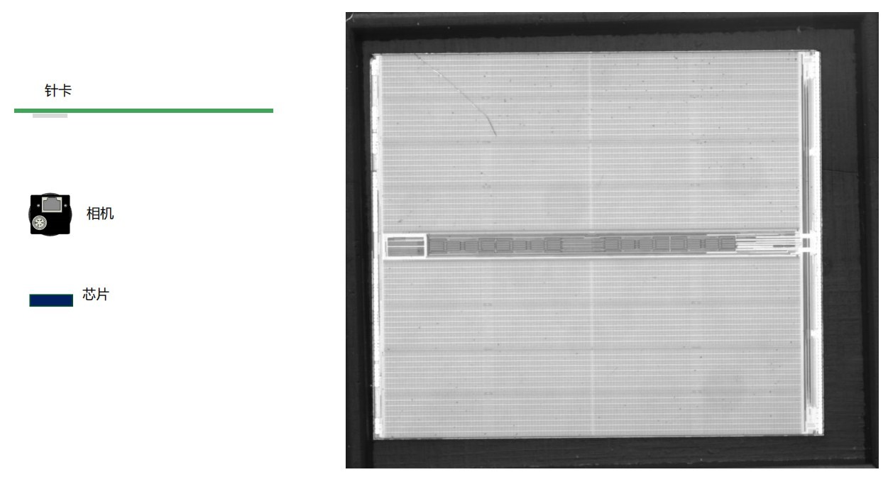
The Boming chip positioning visual inspection equipment can perform full-size detection of wafer probes, chip round holes, and outer R corners, ensuring that unqualified and defective chips are screened out, effectively ensuring the smooth progress of the assembly process of probes and modules, and modules and bases. Its accuracy can reach up to 0.7μm.
Core Advantages

Intelligent
Integrates multiple technologies, powerful hardware and software
(Complete range of standard and customized products)

Advanced Algorithms
Deep Learning defect detection algorithm, model inference (defect segmentation or defect location)
(Background interference removal, defect merging, detected defect screening, etc.)

One-Click Start
One-click detection start, multiple cameras work independently
(Numbered summary of detection results sent)

Automation
Automatic detection, products flow out with the conveyor line, no manual selection required
(Detection workstation optional)
High Precision
High dimensional measurement accuracy, fast speed, high detection efficiency
(Repeat detection accuracy: ±5μm)

Customizable Development
Customizable development according to actual needs,
(Custom Development)
Vision Solution
Positioning Process
Product Positioning Process
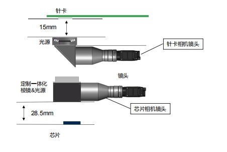
· Adjust the correspondence between the chip and the needle card
· Save the chip image
· Complete the nine-point calibration of the chip
· Use the image saved in step 2 to calculate the basic chip XY position and angle
· Take a picture of the product and calculate the current position
· Move the product to the reference chip position, alignment complete
Overall Layout
It can be used for full-size detection of wafer probes, chip round holes, and outer R corners to ensure that unqualified and defective chips are screened out, effectively ensuring the smooth progress of the assembly process of probes and modules, modules and bases, with an accuracy of up to 0.7μm.


Video Number
Public Account
Douyin Signal
Zhuhai Bomming Vision Technology Co., Ltd SEO Privacy Policy
Business License